Wafer Level Reliability Testing
Contents
Wafer Level Reliability TestingWafer Level Reliability Testing
As semiconductor devices shrink in size and become more complex, it has become necessary for semiconductor fabrication facilities (fabs) to use more parameters to monitor and control production processes. Today, thousands of parameters are being monitored and the number is expanding. Because of these technology trends, fabs are making greater use of a methodology called wafer level reliability (WLR) testing.
WLR testing is a statistical process control tool that gathers data through parametric testing to identify process anomalies that could degrade long-term device reliability. This type of testing applies a high level of stress to special test structures on the wafer and measures the degradation caused by this stress. This testing sometimes takes the structure to the point of failure, but does not affect the rest of the wafer. Based on predetermined test times and stress levels, results can be interpreted to identify sources of anomalous variation in the production process.
The importance of WLR testing is growing because it often helps shorten the startup time of new fabs (now costing $billions) by reducing the amount of traditional stress testing required to qualify new products and processes. It is also used as an ongoing test tool at more than 100 different fabs around the world where a wide variety of devices are produced utilizing MOS, CMOS and bipolar technologies. WLR testing can accommodate virtually any type of semiconductor device and has been instrumental in helping fabs quickly reach targeted yields and other production goals.
WLR shortens test cycles and startup time by reducing a fab's reliance on traditional stress testing done early in the process development cycle. Traditional stress testing takes hundreds or thousands of hours before providing wafer processing results. WLR testing provides reliability information almost immediately because it is conducted on-line in real time.
WLR and Parametric Test Methods
The distinction between WLR and other parametric testing is in the type of data sought and how it is used. Most of the current parametric testing is concerned with process control monitoring to maintain or improve yields. For this purpose, parametric testing gathers data that relates to how semiconductor devices perform immediately after production or after a set of process steps. Simulation of the device under test (DUT) takes place without stress. WLR testing applies a high level of stress to accelerate a DUT's response which can be interpreted statistically to indicate the long-term performance of devices produced on the wafer.
The commonality between both types of testing (WLR and parametric) is in the use of special test structures that are probed to gather data. Both use automated parametric test systems with high-speed algorithms to accelerate data collection. The deliverables that define a WLR testing system consist of two components: the test structures (in the form of a GDS II or CIF design file) and the algorithms for testing these structures.
Yield and reliability problems are often caused by adverse process interactions. WLR testing attempts to identify these interactions by measuring the degradation of electrical parameters. In effect, WLR test data integrates the results of a set of process steps leading up to the point where testing took place to determine if those processes affect device reliability. For this reason, there is a growing trend to use WLR testing as an integral part of online production monitoring at multiple process locations in the fab.
Greater use of WLR testing is a natural extension of the ongoing trend to use more types of parametric testing to help control front end processes. These test programs contribute to a fab's proactive agenda of continuous process improvement. The discovery of process variations (as well as eliminating the sources of these variations) allow potential defects to be identified before they produce defective products. If there is no process variation, then there is only one interaction effect, i.e. the production of good product.
Comparison of Reliability Testing Models
Reliability test models can establish a correlation between WLR test results and traditional reliability stress test data. For example, stress testing conducted early in the product development cycle is used to estimate the failure rate of new semiconductor devices, insuring their ability to meet customers' long-term reliability goals. This type of stress testing takes weeks or months and is not suitable for process monitoring.
WLR testing can be used to measure rate of degradation on the same devices that are subjected to longer term tests. WLR test results are a statistical signature of the rate of degradation of test devices. Subsequent product can then be monitored using only fast WLR tests.
As long as the rate of degradation determined with WLR testing is within statistical distributions of that seen in long term tests, then current product should be expected to have a similar reliability as samples previously subjected to long term tests. However, if the current product lot shows a different rate of degradation, it may not show the same level of reliability that was demonstrated in the initial testing. This material should then be examined to determine the reason for this different rate of degradation (good or bad) and the process corrected to produce the minimum variation.
In functional life tests, finished products are used. This assumes that product samples were selected from a consistent process and that failure mechanisms are primarily related to time dependent stress conditions, such as, applied electric field and temperature. This testing paradigm does not attempt to correlate failure mechanisms with process variables but suggests that corrections take the form of product design changes or application limitations.
There are a number of shortcomings in this type of reliability testing model:
By contrast, WLR testing is focused on time dependent failures with their origins in process variations. This reflects the current maturity of the semiconductor industry and its body of knowledge relating to time dependent failures. The WLR approach begins by developing a thorough understanding of prominent failure mechanisms. With that understanding, test structures and algorithms can be created for multiple processes and failure mechanisms to uncover variations that could lead to long-term reliability problems.
WLR testing requires a combination of sensitive, high-speed parametric measurements and valid test structures. Test structure design must be solidly grounded in physics of failure expertise. Specifically, the creation of structures and algorithms for valid WLR testing requires a partitioning of each failure mechanism into the underlying material and process parameters connected with the failure.
For example, contact/via reliability can be affected by electromigration, junction spiking, stress migration effects, and thin dielectric contamination (all of which are a function of multiple process variables). Therefore, the appropriate test structure set should have multiple devices in order to detect these different failure mechanisms and processing problems. A single contact or via chain would not be sensitive to all these mechanisms.
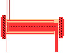
Figure 1. The junction spiking test examines the tendency for aluminum to dissolve silicon from the contacts.
A junction spiking test structure (Figure 1) can be used to examine the tendency for aluminum to dissolve silicon from the contacts. The electromigration test structure (Figure 2) is used to monitor the rate of grain boundary or interface self-diffusion of aluminum. In addition, various contact or via chains should be used to measure the impact of process issues such as step coverage, outgassing of moisture from low density planarization oxide layers, self poisoning effects, or excessive over-etch on specific geometries.
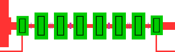
Figure 2. The electromigration test structure is used to monitor the self-diffusion of aluminum in a preferred direction due to momentum transfer from electrons flowing in a metal line.
A test structure is an emulation of an actual semiconductor device or other physical structures that result from a set of process steps
Test structures may be placed on the semiconductor wafers (Figure 3)as drop-ins, which are located where functional die would normally be placed. They could also be placed in wafer scribe lines (referred as "scribe line monitors"), which are lines between functional die defining saw cuts that separate finished die. The latter scheme saves potentially useful wafer real estate for functional devices. On the other hand, using drop-ins greatly increases the opportunity to expand the number and area of test structures, which can provide a more thorough evaluation of the processes being monitored.
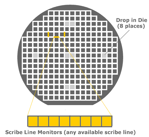
Figure 3. Test structures may be drop-in die or scribe line monitors.
Test structures are probed to execute the WLR test algorithms in a manner similar to other types of parametric tests. Typically, the parametric tester applies a constant DC voltage or current, or a low frequency AC signal through the probe. Then the resulting voltage, current or capacitance is measured. When this is done on a sufficient number of wafers and test sites, a statistical distribution of the measured parameter is obtained.
Test results are used to predict the probability that a particular lot coming though the fab will meet reliability requirements for the devices on the wafer. This is accomplished by comparing the current distribution of test data to the distribution that was obtained on the initial good lots subjected to qualification testing. If current results are outside the range (statistical limits) of prior experience for good lots, then the process engineer must ask why and analyze the process. With this approach, the engineer can make process adjustments aimed at preventing reliability failure, usually without having to resort to another round of 2,000-hour stress testing.
In effect, WLR testing provides a single-point calibration check of the monitored processes. More importantly, it also provides a new program for monitoring devices to insure long-term reliability. Nevertheless, WLR should not be used to qualify new materials or processes. The existing empirical models used for extrapolating failure rates are not sufficiently accurate to extrapolate 20-year lifetimes from 2-second tests. However, WLR tests should be part of any qualification program to insure that interaction effects have not been introduced with the new process.
For example, if a new metal is introduced, the qualification program must prove that the new material is at least as reliable as the old one. The qualification process must also prove that changes required in the metal etch process because of the new material do not introduce other problems. One of these would be excessive consumption of the oxide exposed after extraneous metal is removed, thus causing an interlevel dielectric problem. It must also prove that the new process did not introduce significant levels of mobile ion contamination, and did not cause damage to the gate oxide due to process induced charging. WLR tests can be applied to answer these questions.
From the example above, assume that the new metal process did not change the quantity of interlevel oxide defects, the amount of mobile ion contamination or the reliability of the gate oxide. WLR tests can test this assumption by comparing the results of the fast WLR tests of the new material to the historical data distribution. If the test results have not changed, then the failure mechanism has not been impacted by the new process.
Still, the introduction of a new material is a significant change and a process engineer would like to know the impact of that change. WLR is not a tool for estimating the quantitative effects of a change. However, it can be used to verify that no change has been produced. Thus it tests for interaction effects within the process.
The WLR paradigm offers several advantages over a sample burn-in process monitor. The most obvious and immediate advantage of WLR testing is its ability to supply real-time information. This is a result of using an automatic parametric tester (APT) to collect in-line data. Feedback on process results and their potential impact on reliability are immediately available.
WLR testing also provides a large number of test structures and parameters, not just a failure rate. There is typically no additional failure analysis needed following WLR testing. Burn-in failures require extensive, difficult failure analysis in order to determine the cause of failure.
Burn-in tests are typically impacted by random defects due to the fact that the tested element is a product die and thus has much more area than a small WLR structure. However, the defect density of the product is measured on every wafer of every lot built as part of functional testing. A low yielding wafer or lot is likely to show a higher defect density and thus high product fallout in a reliability test. Defect density monitoring can therefore be done through yield analysis and does not require burn-in.>
To put this in perspective, burn-in tests can uncover defects introduced by assembly processes. WLR tests can not detect such defects. However, monitoring yield loss at assembly is the most effective method of dealing with defect density issues. In addition, a process control program in the assembly area itself (e.g. bond pull tests to examine intermetallic formations of the ball bonds) can be established to detect true wearout failure mechanisms associated with package assembly.
Compared to long-term stress testing WLR provides more data, more quickly, and in greater detail. Also, there is no damage to functional die which occur during burn-in and other tests. Ultimately, WLR in conjunction with yield monitoring should reduce the amount of time and costs associated with lot sample burn-in.
The payoffs in adopting WLR testing include:
A trend that should further accelerate the use of WLR testing is closer cooperation between fabs, automated parametric test (APT) system manufacturers and suppliers of complementary software. Each of these organizations recognizes the need for information from the others to create and get maximum benefits from parametric testing.
Wafer fabs supply information regarding known process sensitivities. The APT system manufacturer supplies knowledge on the best way to test for those sensitivities, using its expertise in the design of instruments, test structures, and algorithms. For example, the test structure designer has to follow design rules of the fab for the wafer under test. Similarly, the APT system manufacturer supplies details on how test algorithms and protocols can be integrated into the fab's process line.
Still, APT/WLR test data must also be integrated into the fab's data base to become part of the plant's entire process history. This requires software specifically designed to make the data available to all those who need it, including process engineers, device designers, circuit designers, test engineers, and those who design test structures. When compared with an existing data base, new data can be used to make adjustments to device designs and fab processes.
The stress-driven, classical reliability methodologies will continue to be used to evaluate new processes and identify new (or variations of) known failure mechanisms. WLR will use the knowledge gained from the traditional tests for the design of new structures for the next generation of wafer processes. WLR will therefore continue to evolve to allow manufacturers to meet the quality levels required in demanding applications.